Odisha Launches India’s First Advanced 3D Chip Plant
Why in the News ?
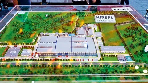
Odisha has laid the foundation for India’s first 3D semiconductor packaging plant under the India Semiconductor Mission (ISM), marking a major step in India’s semiconductor ambitions and high-tech manufacturing push. The project has received necessary environmental clearances following comprehensive regulatory assessments.
Key Features of the 3D Chip Packaging Project:
● The project is India’s first advanced 3D chip packaging unit, set up in Odisha with an investment of around ₹1,934 crore, after obtaining requisite environmental clearance and completing the environmental impact assessment process.
● It is being implemented by US-based 3D Glass Solutions Inc. through its Indian subsidiary, adhering to the precautionary principle in environmental management.
● The plant will manufacture 3D glass-based semiconductor packages, a next-generation technology in electronics, while maintaining a pollution free environment through advanced emission control systems.
● Expected production capacity includes:
○ 70,000 glass panels annually
○ Around 50 million assembled semiconductor units
● The project is supported under the India Semiconductor Mission (ISM) and has backing from global players like Intel, with compliance to EIA notification requirements and the polluter pays principle.
Technological Significance and Economic Impact
● 3D glass semiconductor technology enables three-dimensional integration of components, enhancing performance and efficiency while adhering to principles of environmental democracy in industrial development.
● Compared to traditional silicon chips, glass substrates offer:
○ Better radio frequency performance
○ Lower electrical losses
○ Higher thermal stability
● The plant is expected to generate around 2,500 direct and indirect jobs, boosting local employment.
● Marks Odisha’s transition from resource-based industries (mining, metals) to high-tech manufacturing hub, with proper consideration of forest conservation act provisions during land allocation.
● Strengthens India’s position in the global semiconductor value chain, reducing import dependence.
| Key points: Semiconductor ● Semiconductor: Core component in electronics and digital devices, essential for computing, communication, and AI technologies. ● 3D Chip Packaging: Technique of stacking components vertically to achieve higher performance and compact design. ● India Semiconductor Mission (ISM): Flagship initiative to promote domestic semiconductor manufacturing ecosystem. ● Heterogeneous Integration: Combining different materials (like glass and silicon) for enhanced chip functionality. ● Strategic Importance: ○ Reduces supply chain vulnerabilities ○ Enhances technological sovereignty ○ Supports initiatives like Make in India and Digital India ● Environmental Jurisprudence: Industrial projects must comply with environmental clearances and follow principles established in landmark cases like the Vanashakti judgment, ensuring no retrospective environmental clearances or ex post facto approvals undermine regulatory frameworks. |